Figure 2.
Promise of 2D Materials for Neuromorphic Applications
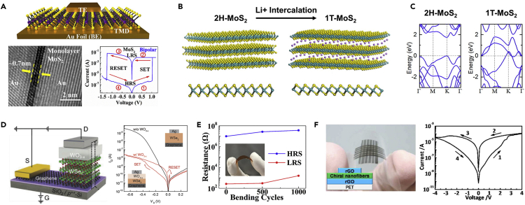
(A) (Top) Schematic illustration of TMD lithography-free and transfer-free sandwich (top and bottom gold electrodes) based on MoS2 grown on Au foil. (Bottom-left) A cross-sectional TEM image of Au/MoS2/Au litho-free device revealing the atomically sharp and clean monolayer interface. (Bottom-right) Representative I-V curve of bipolar resistive switching behavior in a monolayer MoS2 crossbar device. Reprinted with permission from (Ge et al., 2018). Copyright 2018 American Chemical Society.
(B) Phase change behavior of trigonal prismatic 2H-MoS2 to octahedral 1T-MoS2 through Li+ intercalation. Reproduced with permission from (Fan et al., 2015). Copyright 2015 American Chemical Society.
(C) Electronic band structure of 2H-MoS2 (semiconducting) and 1T-MoS2 (metallic). Reprinted with permission from (Gao et al., 2015). Copyright 2015 American Chemical Society.
(D) (Left) Schematic representation of synaptic barristor consisting of vertically integrated WO3–x memristor and WSe2/graphene barristor. (Right) ID-VD curves showing the gate-tunable resistive switching characteristics of the devices with (red line) and without the WO3–x layer (black line). Reprinted with permission from (Huh et al., 2018). Copyright 2018 WILEY-VCH Verlag GmbH & Co. KGaA, Weinheim.
(E) Stable resistance of atomristor device on PET after 1,000 bending cycles at 1% strain with the high-resistance and low-resistance states. Reprinted with permission from (Ge et al., 2018). Copyright 2018 American Chemical Society.
(F) (Left) Snapshot and schematic illustration of 6 × 6 flexible memory devices based on chiral MoS2 nanofibers on PET. (Right) Initial I-V characteristics of a chiral MoS2 nanofiber-based memory cell. Reprinted with permission from (Tan et al., 2015). Copyright 2015 American Chemical Society.

