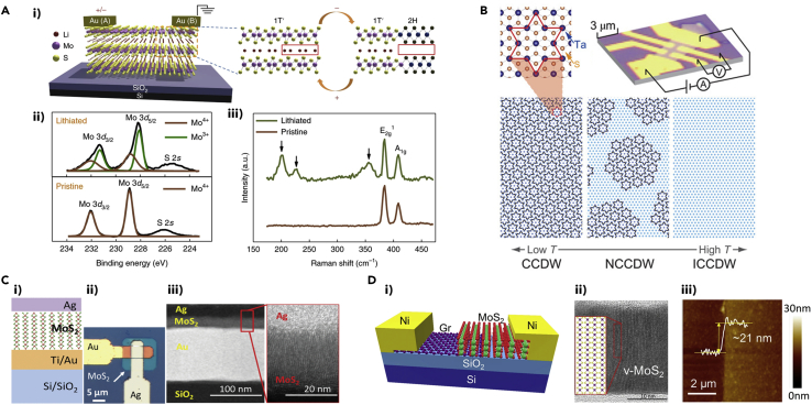
Figure 3.
Representative Images Showing the Working Principles of Synaptic Devices: Phase Change Memristors, Quantum Phase Transition Memristors, and Resistive Memory Devices
(A) (i) Schematic illustration of memristive behavior in MoS2 using electric field-controlled reversible 2H/(1T′) to 1T′/(2H) phase transition controlled by Li+ concentration. (ii) XPS spectra for the lithiated and pristine films. The lithiated film displaying the appearance of Mo3+ peaks indicating conversion of Mo4+ to Mo3+ peaks. (iii) Raman spectra of lithiated and pristine MoS2 films showing additional peaks (marked by arrows) at 200, 225, and 355 cm−1, corresponding to the characteristic peaks of 1T′ MoS2. Reprinted with permission from (Zhu et al., 2019). Copyright 2019 Springer Nature.
(B) An optical microscopic image of a 1T-TaS2 memristive device (top-right) and a schematic illustration of Ta atom network in the CCDW (left), hexagonal NCCDW (middle), and ICCDW (right) phases, with the CCDW phase zoomed-in in the inset. The dark blue dots represent the displaced Ta atoms from their undistorted lattice coordinates, forming David-star clusters. Reproduced with permission from (Yoshida et al., 2015). © The Authors, some rights reserved; exclusive licensee American Association for the Advancement of Science. Distributed under a Creative Commons Attribution NonCommercial License 4.0 (CC BY-NC) http://creativecommons.org/licenses/by-nc/4.0/.
(C) (i) Schematic illustration and (ii) optical microscopic image of the vertical stack MoS2 threshold switching memristor. (iii) Cross-sectional STEM and HRTEM images of the MoS2 memristive device showing vertically aligned 2D MoS2 layers. Reprinted with permission from (Dev et al., 2020). Copyright 2020 IEEE.
(D) (i) Schematic illustration of vertical MoS2/graphene threshold switching memristor. (ii) Cross-sectional HRTEM image of vertically aligned MoS2 at the MoS2/graphene interface. (iii) AFM image revealing MoS2 thickness of ∼21 nm. Reprinted with permission from (Kalita et al., 2019). Copyright 2019 Springer Nature.

