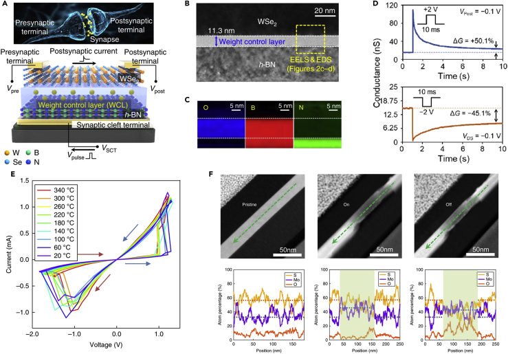
Figure 5.
vdW heterostructures with 2D materials for neuromorphic applications
(A) Schematic illustration of an h-BN/WCL/WSe2 synaptic device.
(B and C) (B) Cross-sectional TEM image of the h-BN/WCL/WSe2 structure, and (C) electron energy loss spectroscopy mapping images of oxygen, boron, and nitrogen showing the heterostructure corresponding to the yellow box in (B).
(D) Conductance trajectories of the excitatory postsynaptic current and inhibitory postsynaptic current when applying pulses with 10 ms width and 2 V amplitude to the WCT. Reprinted with permission from (Seo et al., 2018). Copyright 2018 Springer Nature.
(E) Switching performance of a GMG device at different temperatures. The arrows indicate the switching direction.
(F) In situ cross-sectional STEM images and corresponding EDS line profiles of a single GMG device in the pristine (left), ON state (center), and OFF state (right). EDS line profiles obtained from the region of green arrows in STEM images. Reprinted with permission from (Wang et al., 2018). Copyright 2018 Springer Nature.

