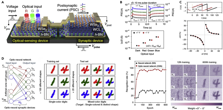
Figure 8.
vdW Heterostructure Optoelectronic Synapses
(A) Schematic illustration of an h-BN/WSe2 synaptic device integrated with h-BN/WSe2 photodetector.
(B) Postsynaptic current characteristics and extracted conductance changing under different light conditions.
(C) STDP behavior obtained from the synaptic device.
(D) ONN for recognition of 28 × 28 RGB-colored images.
(E) (Left) Training and the testing datasets consisting of single-colored and color-mixed numeric pattern images. (Right) Weight mapping images after the 12th and 600th training epoch. Reprinted with permission from (Seo et al., 2018). Copyright 2018 Springer Nature.

