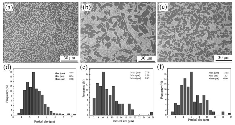
Figure 27.
Optical microscopy images of the microstructure of SLM-processed parts obtained at a laser power of 320 W, (a) contour, (b) middle (contour offset) and (c) central regions and the corresponding dimension analysis of the primary silicon phase (d) contour, (e) middle and (f) central regions [152]. Copyright 2015. Adapted with permission from Elsevier Science Ltd. under the license number 4803730069705 (Figure 3 [152]), dated 7 April 2020.

