
Figure 1.
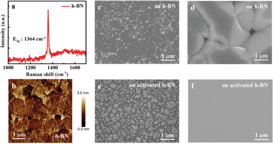
a) Raman scattering spectrum of 3‐nm‐thick annealed h‐BN on Al2O3. b) AFM image of 3‐nm‐thick annealed h‐BN on Al2O3. SEM images of c) 30‐nm‐thick LT‐GaN and d) subsequent 1.5‐µm‐thick HT‐GaN grown on untreated h‐BN/Al2O3 substrate. SEM images of e) 30‐nm‐thick LT‐GaN and f) subsequent 1.5‐µm‐thick HT‐GaN deposited on HCl‐activated h‐BN/Al2O3 substrate. These SEM results indicate that a drastically improved surface of HT‐GaN epilayer owes to the increasing of GaN nucleation density by HCl treatment of h‐BN.