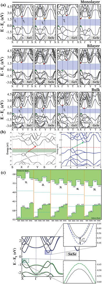
Figure 2.

a) Electronic band structures for monolayer, bilayer, and bulk MMCs (calculated using the Heyd‐Scuseria‐Ernzerhof (HSE06) hybrid functional). Solid circles are VBM and CBM. Black arrows (dashed) are possible direct transitions (T1 and T2) to points very close in energy to the VBM and CBM. Reproduced with permission.[ 31 ] Copyright 2015, American Physical Society. b) Electronic structure of SiS monolayer, calculated using density functional theory (DFT) (left panel). Reproduced with permission.[ 79 ] Copyright 2015, American Chemical Society; SiSe monolayer calculated using HSE06 hybrid function (right panel). Reproduced with permission.[ 64 ] Copyright 2015, American Chemical Society. c) Top panel: Calculated band alignments of MXs of 1–5 layers (L) (at the HSE06 level). Reproduced with permission.[ 80 ] Copyright 2017, Royal Society of Chemistry. Bottom panel: Electronic band structure of SnSe monolayer with (dashed lines) and without (continuous lines) spin–orbit coupling effect. Reproduced with permission.[ 31 ] Copyright 2015, American Physical Society.
