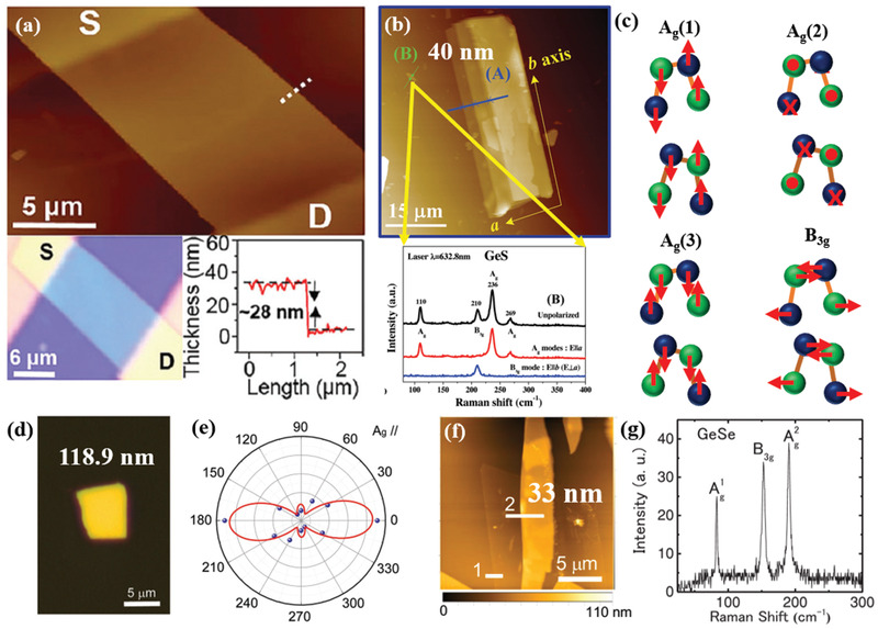
Figure 3.

Mechanically exfoliated GeS and GeSe flakes. a) Atomic force (top panel) and optical microscopy (bottom panel) images. The thickness of the GeS flake is ≈28 nm (along the white dashed line (in top panel)). S and D correspond to source and drain, respectively. Reproduced with permission.[ 66 ] Copyright 2016, Royal Society of Chemistry. b) AFM image of exfoliated GeS flake with a thickness from 40 nm (solid green line B) to three‐step stack of up to about 270 nm (solid blue line A). Polarized Raman spectra of the 40 nm‐thick GeS flake (bottom panel). Reproduced with permission.[ 98 ] Copyright 2017, Wiley‐VCH. c) Schematic representation of the motion of atoms for the different Raman active modes in MXs. d) Optical image of GeSe flake. e) Angle‐resolved polar plot of the Raman peak intensity of Ag mode (188 cm−1, Laser: 532 nm laser under parallel configuration). Reproduced with permission.[ 103 ] Copyright 2019, Wiley‐VCH. f) AFM image with height profile of GeSe (indicate by line 2) and 3L‐MoS2 heterojunction, and g) Raman scattering spectra of a 33 nm GeSe flake (Laser line used: 532 nm). Reproduced with permission.[ 101 ] Copyright 2018, Wiley‐VCH.
