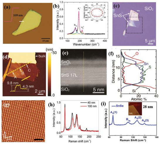
Figure 4.

a) Optical microscopy image of a mechanically exfoliated, 109 nm‐thick, SnS flake on SiO2/Si substrate; the corresponding AFM height profile is shown in the inset. b) Raman scattering spectra of the SnS flake. The solid lines (blue, green, and yellow) are Lorentz‐ fitting curves of the active Raman modes; The angular‐resolved Raman intensity of the mode is shown in the inset. The θ = 0° corresponds to the armchair, x direction of the crystal. Reproduced with permission.[ 50 ] Copyright 2018, American Chemical Society. c) Optical image of exfoliated SnS. d) AFM topography of the selected area in (c). Inset is the height profile along the solid yellow line. e) Cross‐sectional high‐angle annular dark‐field scanning transmission electron microscopy (HAADF‐STEM) image (at the point A in (d)). f) Energy‐dispersive X‐ray spectroscopy (EDS) depth profile along the dashed line in (e). Reproduced with permission.[ 57 ] Copyright 2018, Royal Society of Chemistry. g) Atomic‐resolution noncontact atomic force microscope (nc‐AFM) image of stoichiometric SnSe flake; the inset shows a typical optical image of SnSe2 microdomains on SnSe. h) Raman spectra of the SnSe flake shown in (g). Reproduced with permission.[ 106 ] Copyright 2018, Author(s), licensed under a Creative Commons Attribution 4.0 License, Published by Springer Nature, and i) room‐temperature Raman spectra of SnSe flake. Inset shows AFM height profile along the red line. Reproduced with permission.[ 125 ] Copyright 2017, American Chemical Society.
