
Figure 6.
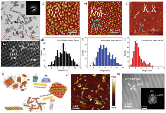
TEM image of a) GeSe sheets (inset: selected area electron diffraction (SAED) pattern taken from a single flake marked by red rectangle), b) high‐resolution transmission electron microscopy (HRTEM) image of a GeSe sheet. c,e,g) Height‐mode AFM images of exfoliated GeSe NSs collected at different centrifugation speed of 3k, 6k, and 9k, respectively (inset: height profiles). d,f,h) Histogram analysis for the thickness of GeSe NSs such as those shown in the panels (c), (e), and (g), respectively. Reproduced with permission.[ 141 ] Copyright 2017, American Chemical Society. i) Schematic illustration of the LPE process used to obtain ultrathin GeSe NSs. j) AFM topography image and height profile of LPE GeSe NSs. k) HRTEM image of exfoliated GeSe NSs in NMP solvent; the inset shows the SAED pattern. Reproduced with permission.[ 142 ] Copyright 2019, American Chemical Society.