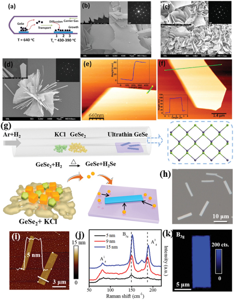
Figure 10.

a) Schematic CVD synthetic process. b–d) Scanning electron microscopic (SEM) images of CVD grown GeSe flakes on the areas indicated by 1, 2, and 3 in (a), respectively (insets: top right corners of (b)–(d) are SAED patterns for representative flakes). The insets panel at the left corners of (b)–(d) are the magnified SEM images. e,f) AFM images of GeSe flakes and corresponding height profile (inset in (e) and (f)) of the flakes (the solid line in (e) and (f)). Reproduced with permission.[ 68 ] Copyright 2013, American Chemical Society. g) Schematic representation of the salt‐assisted CVD with atomic structure of the layered GeSe. h) Optical image of as‐grown GeSe flakes. i) AFM image of GeSe flakes with height profile. j) Raman spectra of GeSe flakes. k) Raman mapping (B3g mode) of GeSe flake. Reproduced with permission.[ 166 ] Copyright 2019, American Chemical Society.
