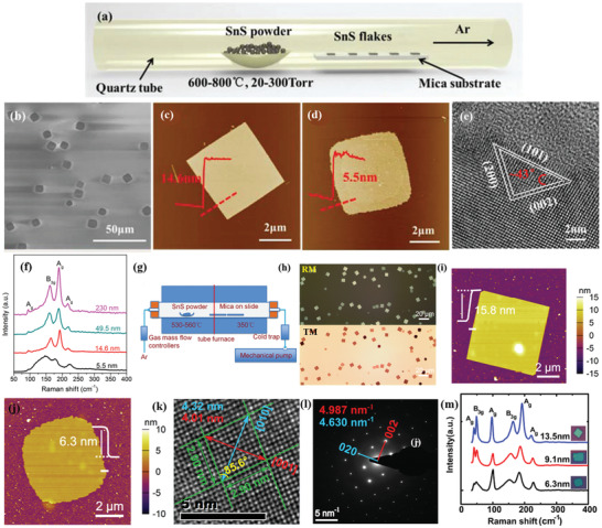
Figure 11.

a) Schematic of PVD growth for anisotropic SnS flakes; b) SEM image of the anisotropic SnS flakes synthesized at 600 °C. c,d) AFM images and height profile of anisotropic SnS flakes. e) HRTEM image of the SnS flake; f) Raman spectra of the SnS flakes with different thicknesses. Reproduced with permission.[ 70 ] Copyright 2016, Royal Society Chemistry. g) Schematic representation of the PVD growth system; characterization of synthesized 2D SnS nanoplates. h) Optical microscopy images on mica substrates (RM and TM correspond to reflection transmission mode of microscopy). i,j) AFM images with height profile. k) High‐resolution TEM image. l) SAED pattern corresponding to the flake shown in (k). m) Raman spectra of SnS nanoplate with different thickness. The corresponding optical microscopic images are shown in the inset. Reproduced with permission.[ 172 ] Copyright 2017, American Chemical Society.
