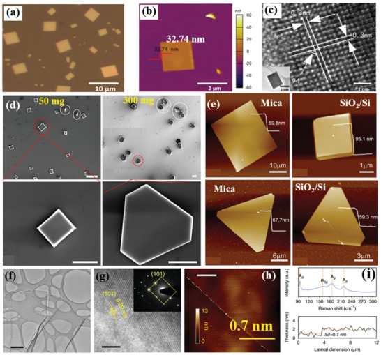
Figure 12.

a) Optical image of SnSe NS on mica substrates (lateral size distribution of 2 to 8 µm). b) AFM image with height profile (inset solid line, height 32.74 nm). c) HRTEM image of a NS (scale bar is 1 nm); a low‐magnification TEM image is shown in the inset. Reproduced with permission.[ 164 ] Copyright 2017, American Chemical Society. d) SEM images of as‐grown flakes on SiO2/Si substrates with 50 and 300 mg Se powders (scale bar: 20 µm (top panel) and 10 µm (bottom panel). e) AFM images of as‐grown and of different shape flakes on mica and SiO2/Si. Reproduced with permission.[ 178 ] Copyright 2018, Elsevier. f) TEM image of SnS monolayer synthesized using a liquid metal exfoliation method. Scale bar is 500 nm. g) HRTEM fringe pattern. Inset: SAED pattern. Scale bar is 5 nm. h) AFM image of the SnS monolayer, and i) Raman spectrum and AFM height profile of the SnS monolayer. Scale bar 8 µm. Reproduced with permission.[ 181 ] Copyright 2020, Author(s), licensed under a Creative Commons Attribution 4.0 License, Nature Publishing Group.
