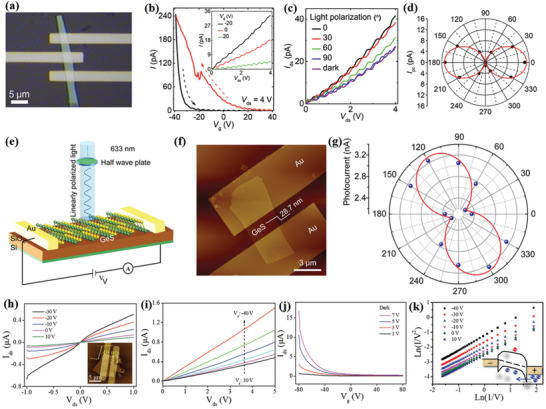
Figure 13.

a) Optical image of fabricated GeS photodetector (45 nm thick GeS); b) gate bias voltage dependent transfer characteristics. Sweeping direction (black and red dotted arrow) indicating the forward and reverse voltage scans, respectively (−40 to +40 V and +40 to −40 V). The inset shows V ds–I characteristics at various back‐gate voltages. c) Incident light (λ = 750 nm) polarization dependent I ds–V ds characteristics of a GeS FET device (P = 32 µW cm−2). d) Polar plots of photocurrent. The angle θ is the polarization direction of the incident light relative to the armchair direction. The solid red curve represents the cos2θ function. a–d) Reproduced with permission.[ 187 ] Copyright 2017, Royal Society of Chemistry. e) Schematic diagram of a GeS phototransistor. f) AFM image of the device (scale bar: 3 µm). and g) polar plot of photocurrent as a function of the polarization angle. e–g) Reproduced with permission.[ 100 ] Copyright 2019, American Chemical Society. h) The I ds–V ds characteristics of a GeSe transistor at different gate voltages. The AFM image of the device and height profile is shown in the inset (thickness and scale bar: 40 nm and 5 µm, respectively). i) Device characteristic curves at different gate bias voltages. j) Transfer characteristics of the device. k) Direct tunneling plots at different gate voltages. The inset shows an illustration of carrier tunneling. Reproduced with permission.[ 188 ] Copyright 2018, Wiley‐VCH.
