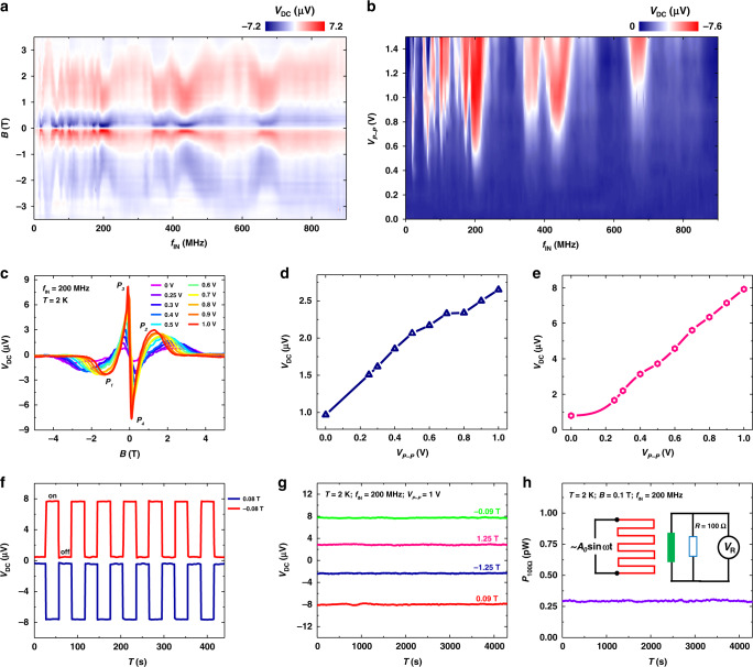
Fig. 5. Manipulating nonreciprocal sensitivity in NbSe2 antenna.
a, Color plot of VDC as a function of the frequency fIN and magnetic field of the NbSe2 antenna device at VP-P = 1 V and T = 2 K. The NbSe2 thickness is five layers. b, Color plot of VDC as a function of frequency fIN and VP-P of the device at B = 0.12 T and T = 2 K. c, VDC-B of the device with VP-P value (that is, the power of the AC signal applied on the resistor) changing from 0 to 1 V at T = 2 K, fIN = 200 MHz. VP1-VP4 are the peak values of VDC. d, e, Extracted VMAX1 and VMAX2 value as a function of VP-P value, where , . Both VMAX1 and VMAX2 values increase monotonically as the increase of VP-P value. f, The dynamic behavior of the device with the AC signal (fIN = 200 MHz, VP-P = 1 V) switching on and off at B = 0.08 T and −0.08 T, respectively. g, Retention behavior of the device under various magnetic fields with a frequency of fIN = 200 MHz, and VP-P = 1 V at T = 2 K. h, Time evolution of the generated power of a 100 Ω resistor connected to the device (B = 0.1 T, fIN = 200 MHz, VP-P = 1 V, T = 2 K), showing a stable detection after 4300 s. Inset, a schematic circuit diagram of the measurement of the generated power on a 100 Ω resistor connected to the device.

