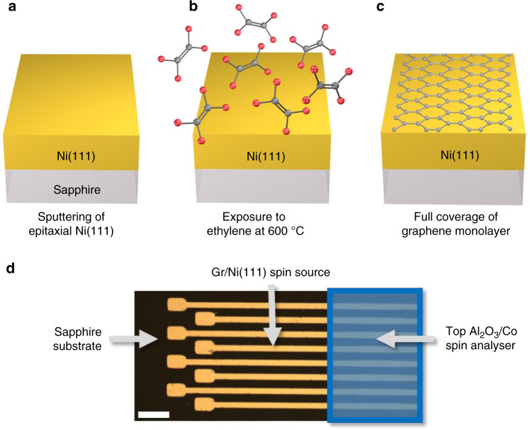
Fig. 1. Schematic illustration of the main steps for the Ni(111)/graphene spin source fabrication.
a Ni(111) is epitaxially grown by a sputtering step at 600 °C on sapphire substrate. b The Ni(111) film is then exposed to a low pressure 600 °C CVD step using ethylene as a carbon precursor. c This results in the full coverage of the Ni(111) electrode with an epitaxial graphene monolayer. d Optical image of the patterned Ni(111)/graphene spin source (scale bar corresponds to 200 µm). A top Al2O3/Co spin analyzer is further deposited on patterned micro-junctions.

