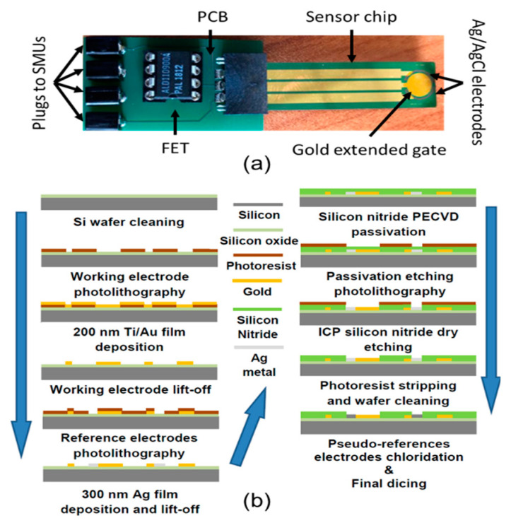
Figure 1.
(a) The sensor chip (10 × 40 mm2 outer dimensions), with the extended-gate gold electrode (sensing area 20 mm2) and two Ag/AgCl pseudoreferences (dark semicircular area around the gold sensing area), connected to the home-made printed circuit board, where the commercial n-type MOSFET ALD110900A is plugged in and four plugs are available to connect the printed circuit board (PCB) with the source-meter units (SMUs). (b) Sketch of the microfabrication process of the sensor chip.

