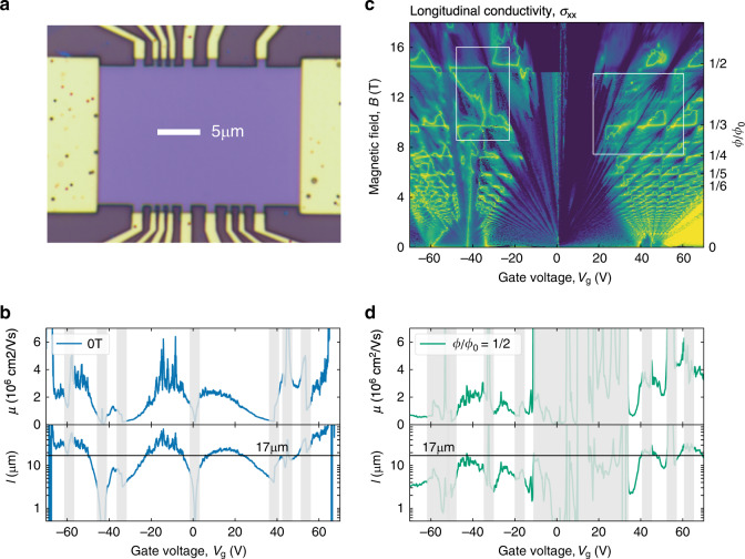
Fig. 1. High-quality graphene superlattices and their transport properties.
a Optical micrograph of one of our devices (D1; twist angle θ between graphene and hBN of about 0.4°). The Hall bar is seen in violet with golden electrical contacts. b Mobility and mean free path for D1 measured at zero B and 10 mK. Semitransparent vertical strips indicate the doping regions around NPs and vHS where n could not be extracted directly from Hall measurements and charge inhomogeneity also plays a role. To calculate μ and l within the shaded regions, we assumed a constant gate capacitance and linearly extrapolated the n(Vg) dependences found sufficiently far from NPs and vHS (Supplementary Note 3). The noisy behavior at large values of μ and l arises from ρxx becoming small (∼1 Ohm, about 4 orders of magnitude smaller than that at the NPs). The horizontal black line indicates the device width W. c σxx(Vg, B) measured by sweeping Vg and varying B in small steps of 40 mT. T = 10 and 250 mK below and above 14 T, respectively. Indigo-to-yellow colors: Log scale truncated between 38 nS and 16 mS for B < 14 T and between 4 nS and 0.4 mS above 14 T. White rectangles: these regions are shown in finer detail in Figs. 3 and 4. d Same as in (b) but for ϕ/ϕ0 = 1/2 (B ≈ 15 T); T = 250 mK. In addition to NPs and vHS, the gray strips also cover a wide region of the quantum Hall regime (|Vg | < 20 V), which is dominated by large cyclotron gaps in the main graphene spectrum. The transport data used to calculate μ and l in (b) and (d) are shown in Supplementary Note 3.

