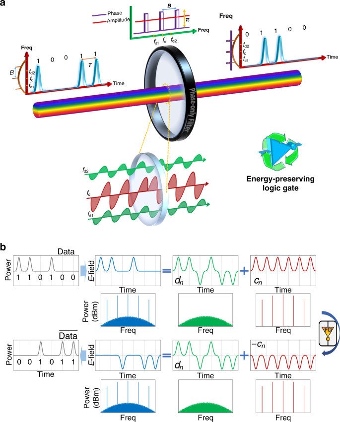
Fig. 1. The operation principle of the proposed frequency-domain zero switching-energy logic NOT gate.
a A frequency-domain (FD), passive NOT gate is implemented using a lossless passive all-pass (phase-only) linear filter. To perform the logical NOT operation on the digital (binary) input data signal, the filter imparts a π phase shift to the clock components of the incoming coherent digital input with respect to the rest of the signal frequency spectrum. Through this process, the output energy spectrum remains unchanged with respect to that of the input signal; however, in the time domain, the logic states of the input bit sequence are reversed. fc (red) shows one of the frequency clock lines and fd1 and fd2 (green) represent arbitrary data frequencies. Note how fc (red) is flipped in orientation at the output of the filter compared to fd1 and fd2. b Conceptual understanding of how amplitude-modulated data streams can be thought of as a sum of their clock, cn (red), and data, dn (green), components. The difference between Data and its inverse, , is a π phase shift (flipping in orientation) on clock frequency tones (red) with respect to the spectral data components (green). The summation of inverted clock frequencies to the original data results in the NOT operation.

