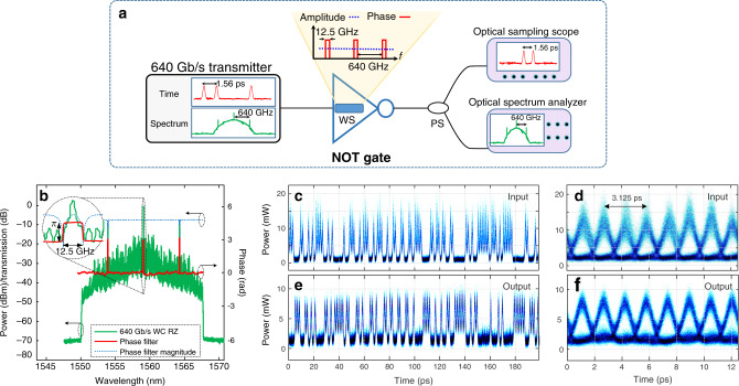
Fig. 4. Proof-of-concept demonstration of the frequency-domain zero switching-energy logic NOT gate.
a Schematic of the experimental set-up. Arrangement consisting of a 640-GHz optical RZ data transmitter, the logic NOT gate, and a receiver to measure the temporal waveform and spectrum of the output signal. The logic NOT gate is implemented using an optical Waveshaper (WS) programmed to produce the needed phase-only linear filtering specifications, i.e., a constant spectral amplitude and a spectral phase profile with π phase shifts periodically spaced by 640 GHz and with each shift extending over a line-width of ~12.5 GHz (determined by the minimum frequency resolution of the WS). b Spectra of the coherent data signal input to and output of the logic gate (they are overlapped), as well as spectral phase profile of the used phase filter (red). c, e Temporal traces of the 640 Gbit/s coherent digital input data signal (c) and the inverted output data signal (e, synchronized with respect to the input for representation purposes). d, f Eye diagram (overlapping the temporal signals over eight consecutive bit time periods) corresponding to the input and output data signals shown in plots c and e, respectively.

