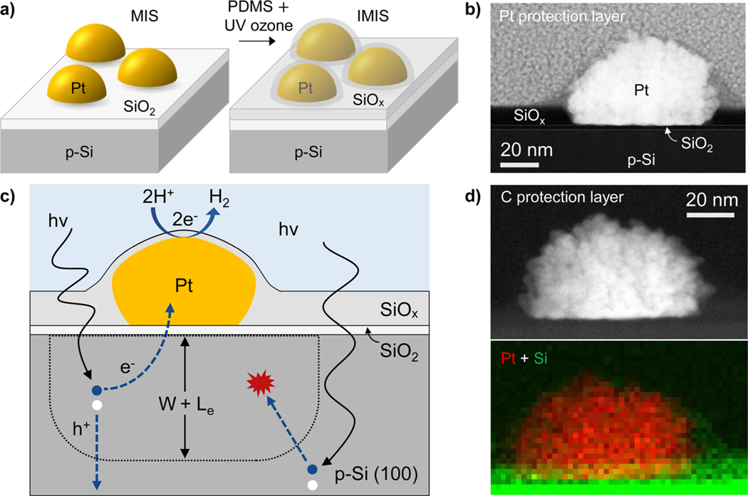
Figure 1.
Nanoparticle-based MIS and IMIS photoelectrodes. (a) Schematic side views of a metal–insulator–semiconductor (MIS) photoelectrode decorated with electrodeposited Pt nanoparticles and an insulator–metal–insulator–semiconductor (IMIS) photoelectrode containing an additional SiOx overlayer. (b) Cross-sectional HAADF-STEM image of a SiOx/Pt/native SiO2/p-Si IMIS nanojunction based on a 10 nm thick SiOx overlayer with Pt protection layer. (c) Schematic side-view illustrating the basic operating processes occurring in an IMIS photoelectrode. (d) Cross-sectional HAADF-STEM image of an IMIS nanojunction described in (b) with a C protection layer (top) and XEDS map of Pt (red) and Si (green) peak signals (bottom).

