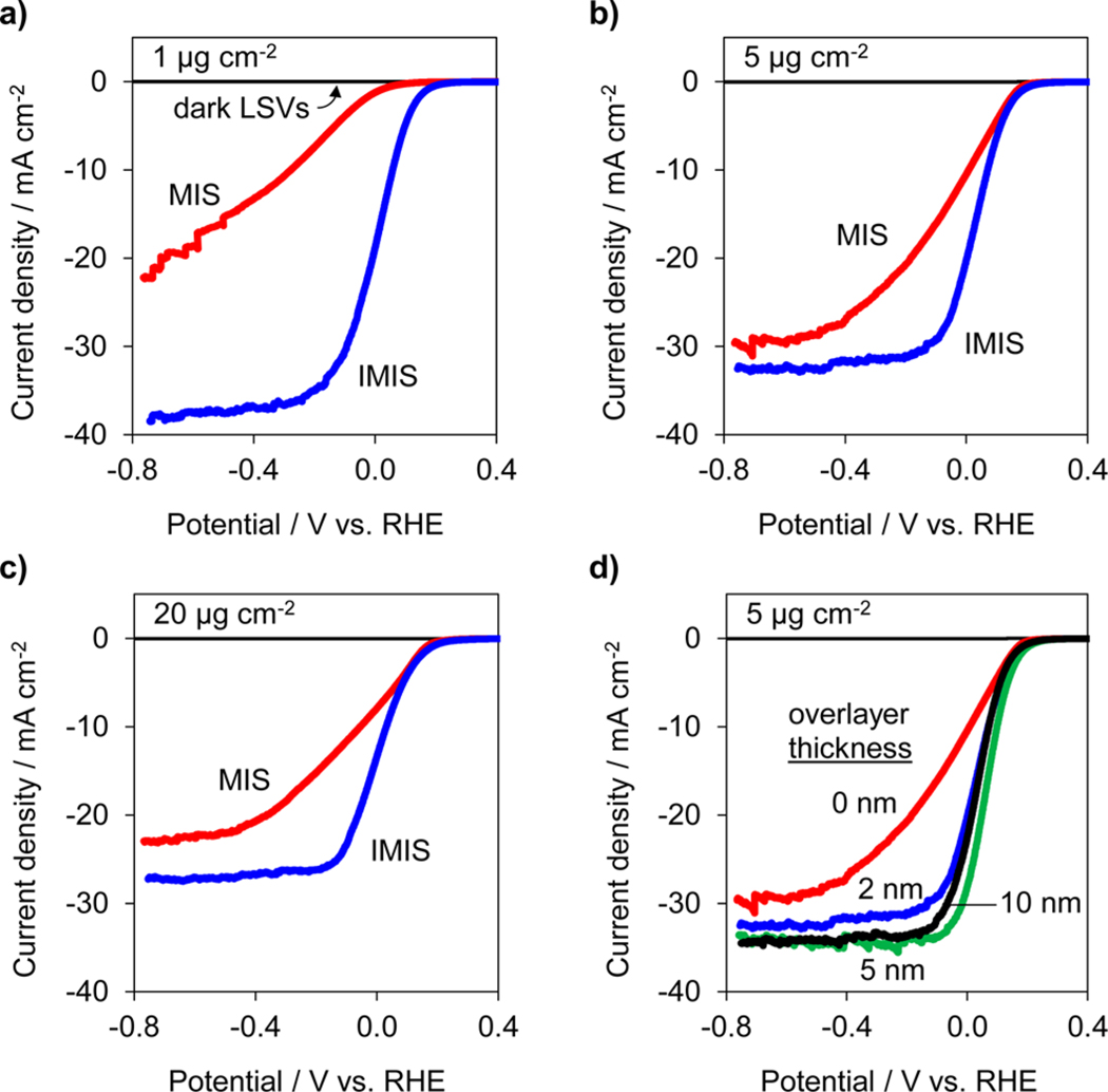
Figure 2.
MIS and IMIS performance. LSV measurements for |Pt| native SiO2|p-Si(100) MIS (red) and |2 nm SiOx|Pt|native SiO2|p-Si(100) IMIS (blue) photoelectrodes for (a) 1 μg cm−2 Pt, (b) 5 μg cm−2 Pt, and (c) 20 μg cm−2 Pt. (d) LSV measurements for |”x” nm SiOx|5 μg cm−2 Pt|native SiO2|p-Si(100) for various SiOx thicknesses from 0 to 10 nm. All LSV measurements were performed at 20 mV s−1 in 0.5 mol L−1 H2SO4 under AM 1.5 G illumination. Current densities are normalized with respect to the geometric area of the exposed photoelectrode.

