Figure 4.
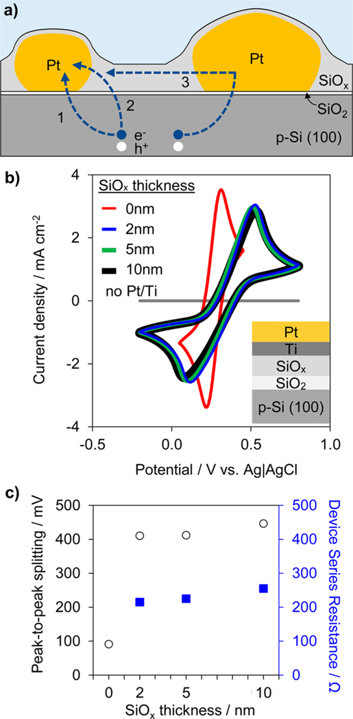
Analyzing carrier transport pathways. (a) Schematic side view of IMIS photoelectrode illustrating possible charge transfer pathways between the Si substrate and Pt nanoparticles. Pathways include (1) conventional tunneling through MIS nanojunction and (2, 3) alternative charge transfer routes involving conduction through the SiOx. (b) CV measurements in 10 mmol L−1 ferri/ferrocyanide, 1 mol L−1 KCl solution for 3 nm Pt/2 nm Ti/“x” nm SiOx/native SiO2/p-Si(100) for various SiOx thicknesses from 0 to 10 nm. The CV sweep rate was 100 mV s−1. (c) Peak-to-peak splitting voltage (circles) and corresponding charge transfer resistances (squares) associated with the CV curves in b.

