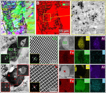
Fig. 1. Microstructures of the CCS annealed at 800°C.

(A) EBSD IPF map. (B) EBSD phase map. (C) BSE image. The BSE image shows the microstructure of the marked region in the phase map, indicating the formation of a dual-nanoprecipitation system: one with lighter contrast and the other one with darker contrast. The IPF map reveals recrystallized (RX) and non-recrystallized (NRX) regions. (D to F) BF TEM image, HR HAADF-STEM image, and EDS maps of the B2 phase, respectively. (G to I) BF TEM image, HR HAADF-STEM image, and EDS maps of the κ-carbide, respectively. SAED patterns [insets in (D) and (G)] indicate the crystal structures of B2 and κ-carbide. DF TEM images taken from the superlattice reflections are shown [insets in (D) and (G)]. FFT patterns [insets in (E) and (H)] confirm the ordered structures of B2 and κ-carbide. The indexes of SAED patterns are shown in the Supplementary Materials and fig. S2. IPF, BSE, SAED, FFT, and EDS refer to the inverse pole figure, backscattered electron, selected area electron diffraction pattern, fast Fourier transform, and energy dispersive X-ray spectroscopy, respectively.
