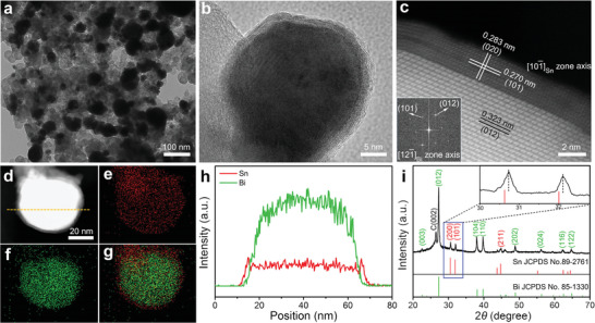
Figure 1.

a) TEM image, b) HRTEM image, and c) HAADF‐STEM image of Bi@Sn NPs. d–g) HAADF‐STEM and EDX elemental mapping images of an individual Bi@Sn NP. h) Line‐scanning profiles of Sn and Bi along the yellow line in (d). i) XRD pattern of Bi@Sn NPs; the corresponding magnified XRD pattern of Bi@Sn NPs is given in the inset.
