Fig. 3.
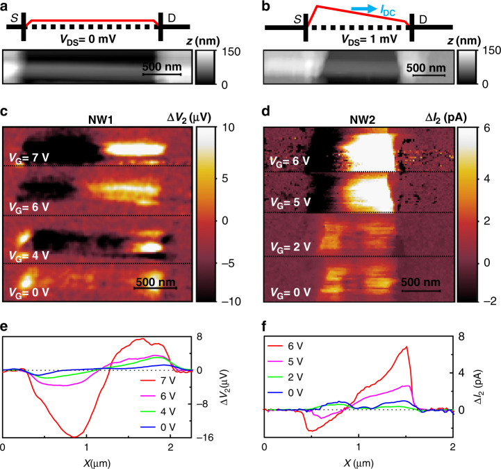
THz near-field photocurrent maps. a, b Sketches of the applied fields on the FET channel of NW1 with an applied VDS = 0 V (a) and of NW2 with VDS = 1 mV (b) together with the topographic maps (in greyscale) of the two FETs. c Near-field second-order photovoltage ∆V2 maps of NW1 with VDS = 0 V and at different gate voltages in the range VG = 0–7 V. d Near-field second-order photocurrent maps ∆I2 of NW2 with VDS = 1 mV and VG in the range 0–6 V. e ∆V2 profiles of NW1 at different VG values as obtained by averaging the horizontal cuts of the maps in panel c over a 50 nm range around the NW1 centre. f ∆I2 profiles of NW2 at different VG values obtained by averaging horizontal cuts of the maps in panel d over a 50 nm range around the NW2 centre. The flat, nearly zero, photocurrent region in panel e reflects the gate-induced screening of the THz field at the centre of the NW

