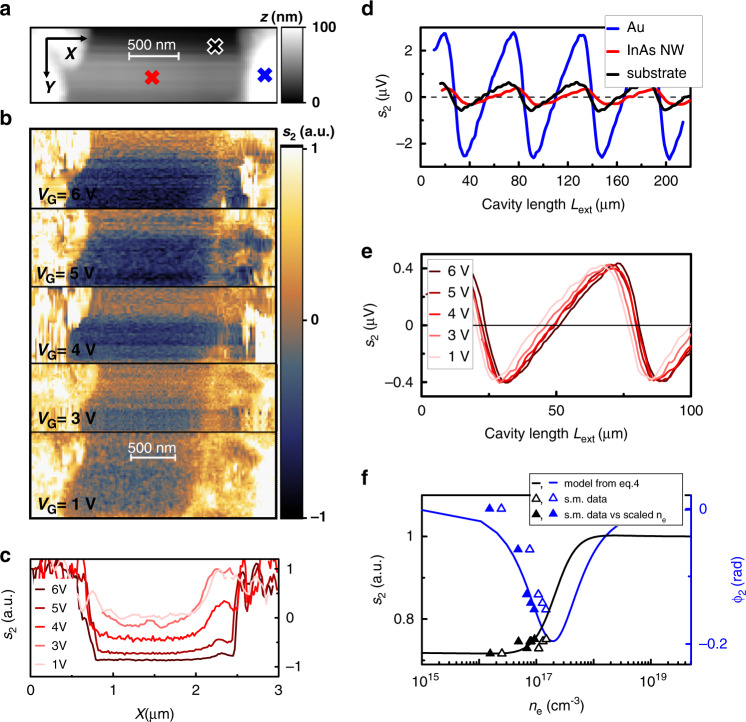
Fig. 5.
Detectorless near-field optical microscopy. a Topography of the NW1 nanowire. b Self-mixing intensity maps demodulated at 2Ω (s2) at different VG values scaled to the substrate value and normalized to the value measured at the gold contacts. The maps are acquired at fixed Lext = 33.5 μm, corresponding to the maximum of the individual self-mixing fringes on gold electrodes. c s2 line profiles obtained by integrating horizontal cuts of the s2 maps in a 50 nm range around the NW1 centre and at different VG values. d Self-mixing fringes as a function of the external cavity length Lext at VG = 0 V. Individual curves correspond to different positions on the sample, marked as coloured crosses in panel a: blue for the gold electrode, red for NW1, and black for the substrate. e Self-mixing fringes acquired at a fixed position on NW1 as a function of the external cavity length Lext for different gate voltages VG. f Amplitude s2 (black) and phase φ2 (blue) of the second-order demodulation self-mixing signal of panel e as a function of the carrier density ne estimated from the transconductance curve assuming a constant mobility (open triangles), together with the predictions of Eq. (4) (solid lines). The experimental s2 values are scaled by a factor of 0.55 μV−1 to match the model at VG = 1 V. Better agreement between the experiment and model is observed for carrier densities ne scaled by a factor of 1.6 (full triangles)

