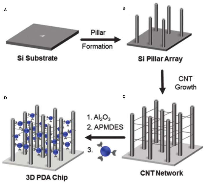
Figure 2.
Schematic illustration of the fabrication of the 3D networked PDA sensor. Reprinted with permission from Lee et al. (2019a). (A) A p-type silicon subsrate. (B) Micropillar structures were prepared on a p-type silicon (100) substrate by a silicon deep etching process. (C) Networked carbon nanotubes (CNTs) were fabricated. (D) The 3D CNT networked pillared structures were coated with Al2O3 using an atomic layer deposition method. Copyright 2016, Royal Society of Chemistry.

