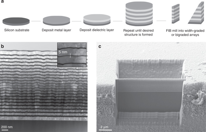
Fig. 4. Fabrication of MIM multilayer arrays.
a Schematic illustration of the fabrication process. b TEM image of a symmetric sputter deposited alternating-layer array structure with central groove width of 5nm shown in the inset. The silver and magnesium fluoride layers are light grey and black, respectively. c SEM image of a cross sectional slice of the same layered structure milled using FIB. The excavated regions on both sides of the device provide free space boundaries at both ends of the grooves

