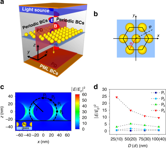
Fig. 2. Optical properties of 2D AuNP lattice.

a Schematic representation of the simulation workspace consisting of plane wave source, plasmonic nanostructure, dielectric substrate (SiO2 glass), photodetectors and appropriate BCs. Linearly x-polarized EM wave propagates through the 2D AuNP lattice. The transmitted photons are collected by a PD on the opposite side of the workspace, whereas the E-field intensity distribution is worked out by placing several PDs in correspondence of the lattice (not all depicted in the sketch). b Top view sketch of the simulation unit cell; the centers of the spherical AuNPs belong to the plane z = 0. The parameters a and φ are the lattice constant and the azimuthal angle, respectively. c Example of E-field distribution normalized to the incident radiation worked out in the plane y = 0 for x-polarized EM plane wave incident on a lattice made of AuNPs with diameter 50 nm and interparticle distance 20 nm. The points P1–P4 are at a distance of 10 nm from the nanoparticle surface at polar angle θ = 0°, 30°, 60°, and 90°, respectively. d Gain of the E-field intensity as a function of AuNP diameter (interparticle distance).
