
Figure 1.
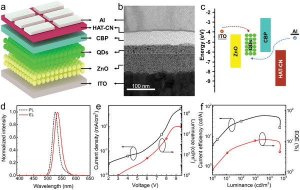
a) Schematic device structure, b) cross‐sectional TEM image, and c) energy band diagram in the unbiased condition of the control device. d) Normalized EL/PL spectra, e) J–V–L, and f) CE–L–EQE characteristics for the control device.
Official websites use .gov
A
.gov website belongs to an official
government organization in the United States.
Secure .gov websites use HTTPS
A lock (
) or https:// means you've safely
connected to the .gov website. Share sensitive
information only on official, secure websites.
a) Schematic device structure, b) cross‐sectional TEM image, and c) energy band diagram in the unbiased condition of the control device. d) Normalized EL/PL spectra, e) J–V–L, and f) CE–L–EQE characteristics for the control device.