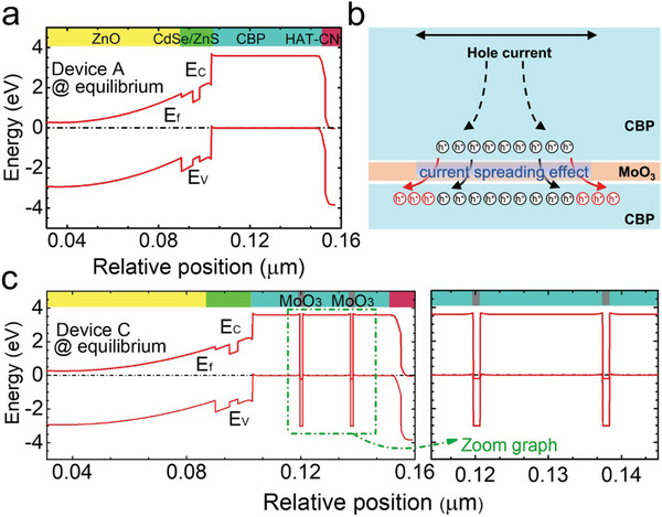
Figure 3.

Energy band diagrams for a) device A at the equilibrium state. b) Schematic diagram of current spreading at the CBP/MoO3/CBP interface. c) Energy band diagrams for device C the equilibrium state. E c, E v, and E f represent the conduction band, the valance band, and quasi‐Fermi level, respectively.
