Figure 5.

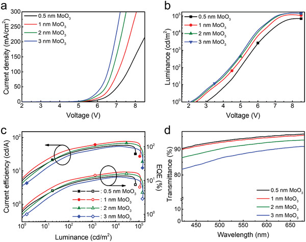
a) J–V, b) L–V, c) CE–L–EQE, and d) transmittance characteristics of the devices with an HTL structure of CBP (16.7 nm)/MoO3 (x nm)/CBP (16.7 nm)/MoO3 (x nm)/CBP (16.7 nm), for which x varies from 0.5 to 3 nm.

a) J–V, b) L–V, c) CE–L–EQE, and d) transmittance characteristics of the devices with an HTL structure of CBP (16.7 nm)/MoO3 (x nm)/CBP (16.7 nm)/MoO3 (x nm)/CBP (16.7 nm), for which x varies from 0.5 to 3 nm.