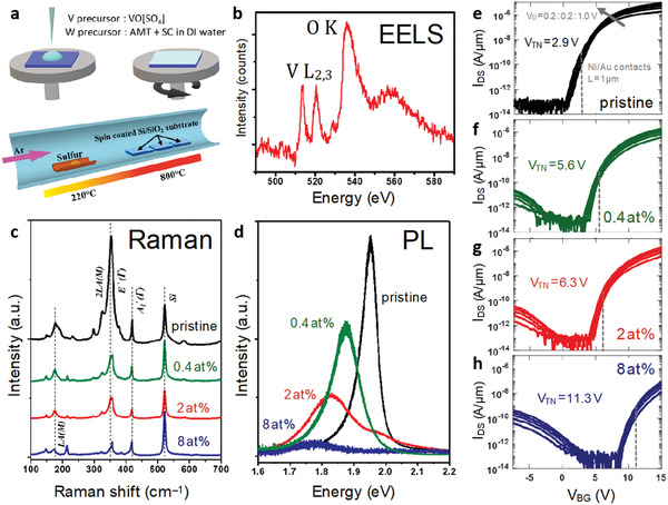
Figure 1.

a) One‐step synthesis of monolayer V‐doped WS2, optical and electronic properties, as described schematically, b) yields a TEM/EELS spectrum with a prominent vanadium L2,3 edge. c) A loss of double resonance in Raman (under 532 nm excitation) and d) pronounced change in photoluminescence response reflect a change of electronic structure as a function of V doping. e–h) Back‐gated V‐doped WS2 field‐effect transistors were fabricated on a 50 nm thick Al2O3 substrate with a Pt/TiN/p++ back‐gate electrode for each doping level. Drain current (I DS) versus back‐gate voltage (V BG) (obtained for drain voltages from 0.2 to 1 V in 0.2 V steps) show a steady shift in threshold voltage across different doping levels and achieve close‐to‐symmetric ambipolar conduction in heavily doped WS2.
