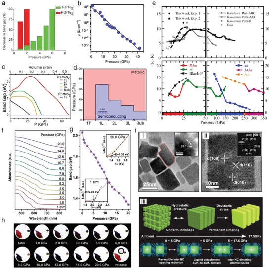
Figure 10.

Optimized optoelectronic properties. a) The calculated bandgap change of T‐ and H‐ZrTe2 with the increase of pressure.[ 201 ] b) Resistivity as a function of pressure for MoSe2. c) Bandgap changes versus pressure in various MoS2 polytypes. d) Pressure‐induced phase transitions in various MoS2 polytypes. e) Several experimental and calculated critical temperature (T c) of phosphorus under high pressure. f) Pressure‐dependent UV–vis absorption spectra of 2D Cs3Sb2I9 perovskite. g) The pressure‐dependent bandgap of 2D Cs3Sb2I9, where the inset describes the bandgap Tauc plots at 0 and 20 GPa. h) Optical images of 2D Cs3Sb2I9 under various pressures. i) Pressure‐induced synthesis of 2D CsPbBr3 perovskite nanoplates. a) Reproduced with permission.[ 201 ] Copyright 2015, Royal Society of Chemistry. b) Reproduced with permission.[ 20 ] Copyright 2015, Springer Nature. c,d) Reproduced with permission.[ 18 ] Copyright 2014, American Chemical Society. e) Reproduced with permission.[ 32 ] Copyright 2017, American Physical Society. f–h) Reproduced with permission.[ 43 ] Copyright 2020, Royal Society of Chemistry. i) Reproduced with permission.[ 226 ] Copyright 2017, Wiley‐VCH.
