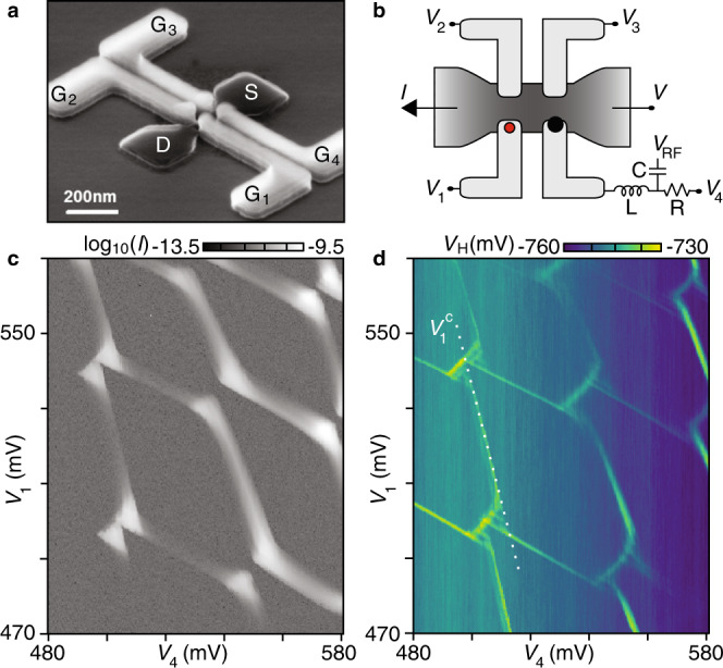
Fig. 1. Compensated control voltages within a two-dimensional silicon quantum-dot array.

a Foundry-fabricated undoped silicon channel connected to reservoirs (dark gray), with four gate electrodes (light gray). This SEM image shows a device from a different fabrication run without backend16. b Device schematic for the example of a few-electron double dot underneath gates G1 and G4, induced by appropriate control voltages V1–4. Each of the three qubit dots (dot 1 indicated in red) capacitively couples to the sensor dot (black), which can be monitored using RF reflectometry off an inductor (L) wirebonded to G4. c, d Charge stability diagram of the double quantum dot in b, acquired at fixed source–drain bias V = −3 mV. Source–drain current I and demodulated reflectometry voltage VH measured simultaneously as a function of V1 and V4. The dotted white line defines a compensated voltage that controls the chemical potential of dot 1 without affecting the chemical potential of dot 4. Control voltages for other dot configurations are established analogously.
