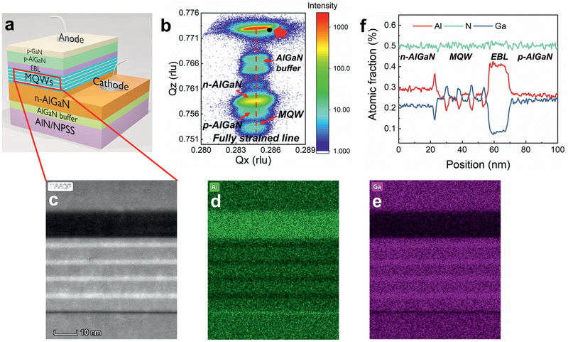
Figure 2.

a) Schematic diagram of the UVC LED structure grown by MOCVD on AlN/NPSS template. b) XRD RSM of the as‐grown UVC LED wafer. The red dashed line presents the reciprocal space position which is fully strained to the AlN template (without relaxation). c) HAADF‐STEM image of the MQWs in UVC LED, the corresponding EDS mapping of d) Al and e) Ga elements and f) the EDS line scan curve is also presented to give a quantitative description of the Al composition distribution. It shows 4 periods of MQW emitting region consisting of approximately 2 nm‐thick Al0.40Ga0.60N wells and 5 nm‐thick Al0.52Ga0.48N barrier layers.
