
Figure 1.
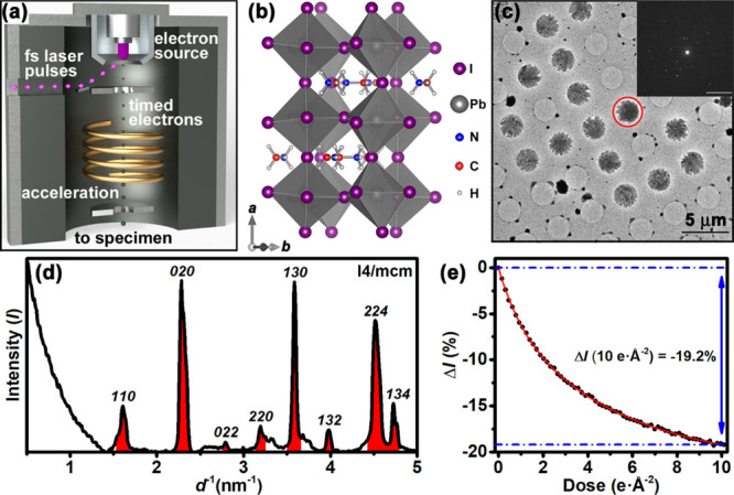
Laser-driven pulsed-beam TEM and quantification of damage to MAPbI3. (a) Simplified schematic of the electron-source region with pertinent aspects and components labeled. Adapted with permission from VandenBussche, E. J.; Flannigan, D. J. Nano Lett.2019, 19, 6687–6694. Copyright 2019 American Chemical Society. (b) Structure of MAPbI3.21 Crystallographic axes are shown in the lower left of the panel. (c) Low-magnification bright-field image of the TEM specimens. The diffraction pattern (inset; scale bar = 5 nm–1) was obtained from the red circled region. (d) Intensity plot from azimuthally averaging the pattern in (c). Red peaks are those used for monitoring beam-induced intensity changes. The space group used for indexing was I4/mcm, though the structure is not yet universally agreed upon.22,23 (e) Bragg-intensity fading curve for a pulsed electron beam (dose rate = 0.001 e·Å–2·s–1; beam size = 245 ± 3 μm2; 50.4 ± 1.0 e/p; f–1 = 2 μs). The red curve is used to determine ΔI at 10 e·Å–2, which here is −19.2%.