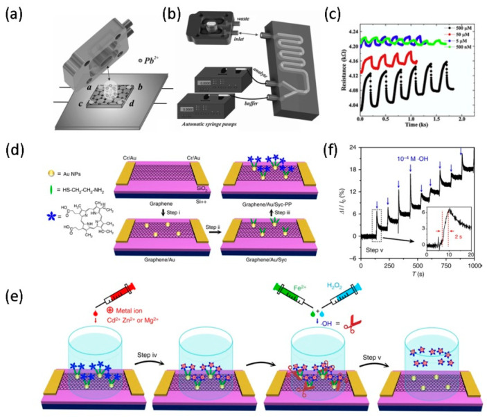
Figure 5.
Diagram of the internal structure of the microfluidic chip (a) and the entire experimental equipment (b). (c) Sensor signals corresponding to different Pb2+ concentrations as a function of time. Reproduced from [41] with the permission from Elsevier. (d) Schematic diagram of the manufacturing process of a field-effect transistor (FET) sensor. (e) Schematic diagram of FET sensor •OH detection. (f) the real-time response signal of the microfluidic FET sensor after adding •OH. Reproduced from [96] with the permission from Nature Publishing Group.

