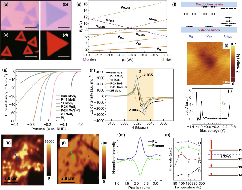
Fig. 18.
Defect-driven properties of 2D materials. a, b Optical images and c, d corresponding fluorescence images of monolayer CVD grown WS. Adapted with permission from Ref. [144]. Copyright 2013, ACS Publications. e Chemical potentials to create point defects elucidated in Fig. 16a, indicate which defects are more likely to occur and f the corresponding schematic of the electronics structural in-gap defect states. Adapted with permission from Ref. [141]. Copyright 2013, ACS Publications. g, h Electrochemical characterisation of various defective MoS2 compared with Pt and the corresponding electron spin resonance with a higher intensity for samples with less sulphur vacancy defect. Adapted with permission from Ref. [148]. Copyright 2016, ACS Publications. i, j STM image of a twin boundary defect and its STS showing an in-gap state at − 0.94 V. Adapted with permission from Ref. [161]. Copyright ACS Publications. k PL enhancement and l Raman quenching at a 1D crack defect in MoS2 and m the corresponding spectra. Adapted with permission from Ref. [162]. Copyright 2014, ACS Publications. n Raman intensity of A′1(Γ) phonon mode of CVD grown WS2 monolayers at four different temperatures (T1–T4). Samples are synthesised with increasing defect densities showing distinct Raman intensities and excitonic energy differences. Adapted with permission from Ref. [138]. Copyright 2019, ACS Publications

