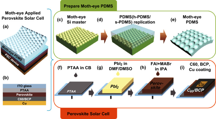
Fig. 1.
Representative schematic images of a completed PSC with moth-eye layer and b PSC configuration. c Fabrication of the hexagonally packed moth-eye array on a silicon wafer. d Replication of the master structure by successive coating and thermal curing of h-PDMS and s-PDMS. e Completed moth-eye PDMS film. f Spin-coating deposition of PTAA hole transport layer on ITO/glass substrate. g Spin-coating deposition of PbI2 thin film. h Fabrication of perovskite layer by additional spin-coating of FAI/MABr/MACl solution in IPA. i Deposition of C60/BCP electron transporting layer on Cu metal electrode

