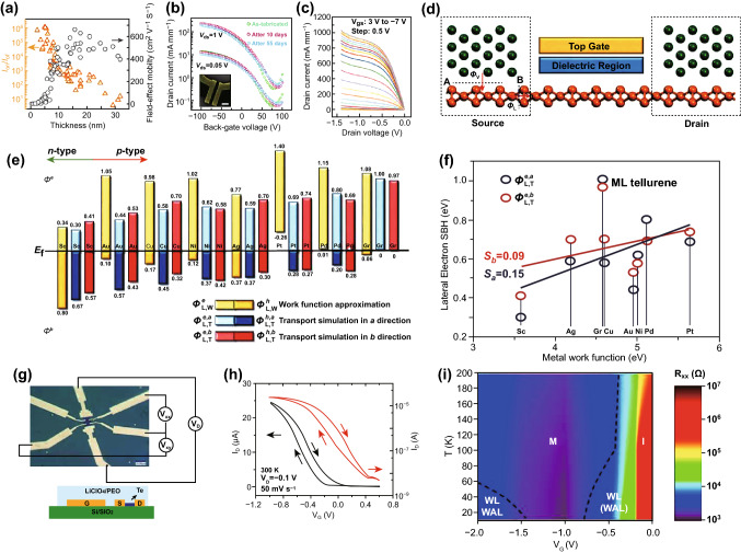
Fig. 12.
a Measured on/off ratio and field-effect mobility of transistors based on 2D Te as a function of thickness. b Transfer curves of the 15-nm-thick Te-based transistor. Inset: SEM image of the 2D Te-based transistor. c Output curves of the 2D Te-based transistor with a thickness of 11.1 nm and a channel length of 300 nm. Adapted with permission from [25]. Copyright 2018, Nature Publishing Group. d Schematic of monolayer Te-based FETs. e Lateral Schottky barrier height (SBH) comparison of the monolayer Te-based FET. f Lateral electron SBH comparison versus the metal work function in the A and B direction (from part d) for the monolayer Te-based FETs. Adapted with permission from [174]. Copyright 2018, The Royal Society of Chemistry. g Optical microscopy image and schematic side-view of a 2D Te-based EGT. h Transfer curves of the device at 300 K. i Gate-voltage-dependent electronic phase diagram of the Te-based EGT. Adapted with permission from [175]. Copyright 2019, American Chemical Society

