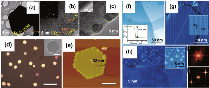
Fig. 3.
a, b TEM and high-resolution TEM (HRTEM) images of a 2D Te flake. Inset of b shows the electron diffraction pattern. c HRTEM image of the Te flake edge. d Optical microscope (OM) image of 2D Te flakes, scale bar = 4 μm, with inset of a single flake. e AFM image of 2D Te flake, scale bar = 2 μm, with the step height profile of the flake edge. Adapted with permission from [67]. Copyright 2014, American Chemical Society. f STM image of 2D Te grown on graphene with a step height profile of the edge. g High-resolution STM of monolayer Te flake. h STM image of the reconstructed graphene (upper and inset) and single-layer Te flake (lower). i, j Fast Fourier transforms of graphene and single-layer Te flake. Adapted with permission from [68]. Copyright 2017, American Chemical Society

