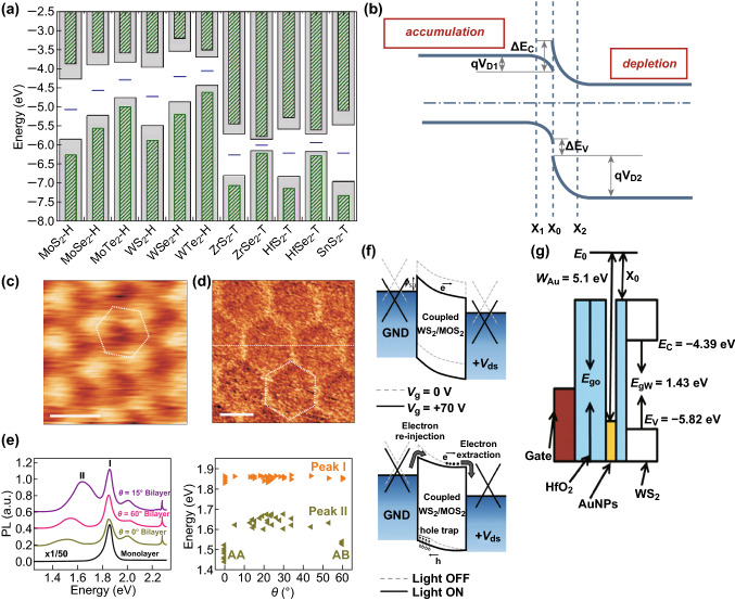
Fig. 3.
Band alignment and band engineering methods. a Theoretical positions of VBM and CBM of VIB- and IVB-TMDs calculated by PBE-SOC. Reprinted with permission from Ref. [33]. b Schematic diagram of band bending at the interface, forming a notch on the accumulation side and a peak on the depletion side. c, d STM measurements of hBN/graphene heterostructure stacked with the different rotation angle of 5° (c) and 0° (d). Reprinted with permission from Ref. [41]. e PL spectra of MoS2 monolayer and bilayers with different twist angles, where peak I is related to the direct transition at K− valley and peak II may be associated with the indirect band gap. Reprinted with permission from Ref. [41]. f The principle of photogating band alignment engineering. Reprinted with permission from Ref. [42]. g The band structure of a floating-gate device based on monolayer WS2. Reprinted with permission from Ref. [43]

