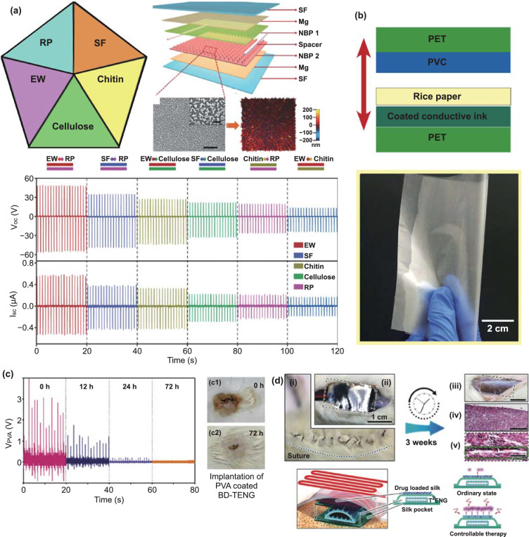
Fig. 4.
a NBPs obtained from wide raw material sources and structure diagram of a typical BN-TENG device: scanning electron microscopy (SEM) and atomic force microscopy (AFM) images of nanostructure on the surface of NBP film. Lower and upper scale bars: 5 and 1 µm. Reprinted with permission from Ref. [89]. Copyright (2018) Wiley-VCH Verlag GmbH & Co. KGaA, Weinheim. b Photograph of the rice paper and scheme of the TENG: PET, PVC, transparent conductive electrode, and rice paper. Reprinted with permission from Ref. [90]. Copyright (2019) Published by Elsevier Ltd. c Electrical output of BD-TENG encapsulated in PVA. (c1, c2) Photograph of the implant site of PVA-coated BD-TENG. (c1) Right after implantation. (c2) 72 h after implantation. Reprinted with permission from Ref. [88]. Copyright (2016) AAAS. d In vivo exhibition of T2ENG’s multiple functions, such as total biodegradation, energy harvesting, biomechanical sensing, and medical therapy. Reprinted with permission from Ref. [96]. Copyright (2018) Wiley-VCH Verlag GmbH & Co. KGaA, Weinheim

