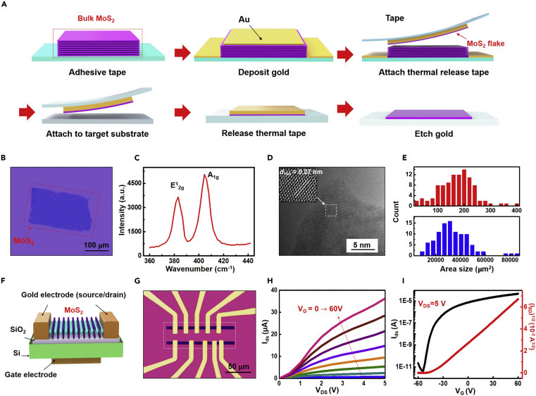
Figure 2.

Transfer process and characterization of an exfoliated large-area MoS2 flake transistor
(A) Schematic illustration of the gold-mediated exfoliation process.
(B) Optical image of an exfoliated MoS2 flake with a lateral size of ~200 × 100 μm on a SiO2/Si substrate.
(C) Room-temperature Raman spectrum of MoS2 showing the A1g mode at 408 cm−1 and the E12g mode at 385 cm−1.
(D) High-resolution TEM image of the atomic layer of MoS2. Inset is the zoom-in view exhibiting a lattice d100 of 0.27 nm.
(E) Histogram comparing flake area size between traditional mechanical exfoliation (in red) and the gold-assisted exfoliation method (in blue).
(F) 3D schematics of the back-gated FET device on the SiO2/Si substrate.
(G) Optical image of the MoS2 FET device from the top. Different channel lengths were fabricated for optimization of the design.
(H) Output curve (source-drain current IDS versus source-drain voltage VDS) with the back-gate voltage VG sweep from 0 to 60 V.
(I) Transfer curve (IDS as a function of VG) with VDS = 5 V, shows n-type behavior with an on/off ratio of 107.
