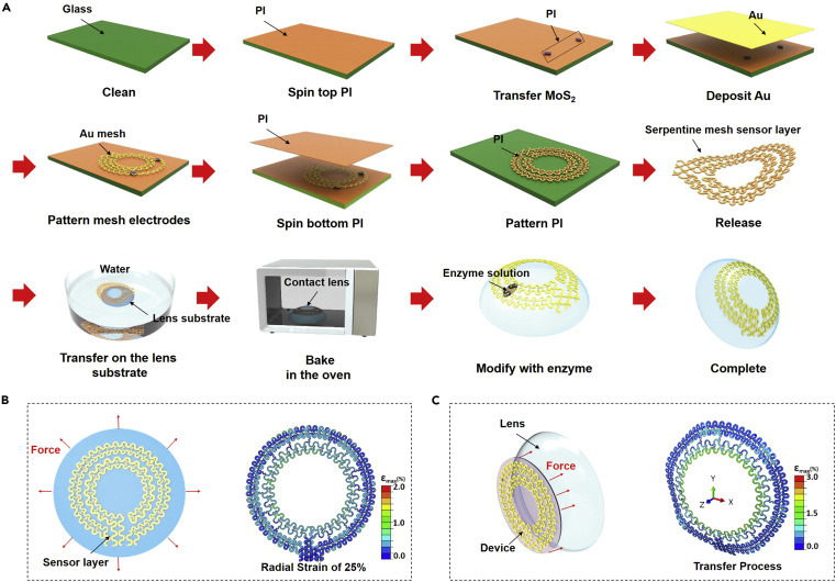
Figure 3.

The “pattern-release-transfer” process and mechanical analysis of a smart contact lens
(A) Illustration of the fabrication process of a smart contact lens. We began by coating the bottom PI layer on a glass substrate. The MoS2 and gold mesh electrodes were consecutively placed and patterned to form the sensor and the interconnect layer. Subsequently, the top PI layer was coated and patterned, followed by release from the glass substrate. Finally, the device was picked up by the PDMS contact lens, oven baked, and enzyme modified to complete the process.
(B) Illustration for the sensor layer with the radial strain (x, y axis) (left) and the FEA strain map under a radial strain of 25% (right).
(C) Illustration of the sensor layer with the longitudinal strain on the perpendicular plane (z axis) (left) and the FEA strain map with 4 mm of z axis displacement (right).
