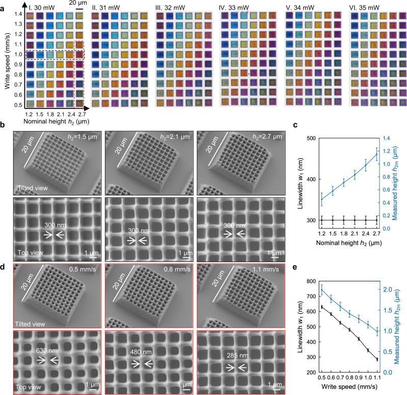
Fig. 2. Optical and scanning electron micrographs (SEM) of as-printed structures.
a Optical transmittance micrographs of a printed colour palette for a constant pitch of 2 μm but varying write speed and nominal height h2 for a range of laser power (I–VI laser power 30–35 mW respectively). b SEM images of grid structures with different nominal height h2 for constant write speed of 1 mm/s and laser power of 30 mW. c Measured grid linewidth w1 and height h2m as a function of nominal height; d SEM images for grid structure with different write speeds for fixed nominal height of 2.7 μm and laser power of 30 mW. e Measured grid linewidth and height as a function of write speed. Values in c and e represent mean and the error bars represent the standard deviation of the measured values (n = 5).

