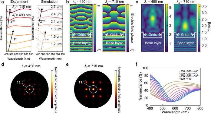
Fig. 3. Finite difference time domain (FDTD) analysis of the grid structure.
a Measured and FDTD simulated transmittance spectra of structures with different nominal height h2 (from the black dashed rectangle in Fig. 2a ranging from 1.2 μm to 2.7 μm. 1st and 2nd represent the first and second order resonance dip respectively). Marked positions λ1 = 490 nm and λ2 = 710 nm are used for FDTD field analysis in Fig. 3b–e. b, c Cross section view of near-field normalised electric field phase and amplitude for a grid structure (laser power: 30 mW, write speed: 1 mm/s, nominal grid height: h2 = 2.7 μm) at dip transmittance 490 nm and peak transmittance 710 nm wavelength respectively (|E/Einc| represents the normalised electric field amplitude). d, e Top view of far-field normalised electric field amplitude for the above grid structure at dip transmittance 490 nm and peak transmittance 710 nm wavelength respectively; the white circle represents collection field for the microscope used in this work (NA = 0.2, CA = 11.5°). f Simulated transmittance spectra for structures with different linewidth w1 (the colours of the spectrum lines were mapped from the corresponding spectra).

