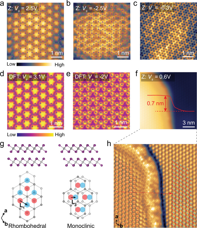
Fig. 3. STM measurements of G/FL-CrI3/Gr.
a–c Bias-dependent STM images of G/FL-CrI3/Gr. STM images taken at (a) Vs = 2.5 V and (b) at Vs = −2.5 V with the superimposed atomic structure of ML-CrI3 (I atoms on the bottom atomic plane are removed for clarity). STM images taken at (c) Vs = −0.3 V. The tunneling current is It = 1 nA. d, e Simulated STM images taken at (d) Vs = 3.1 V and (e) Vs = −2 V with the superimposed atomic structure of ML-CrI3. f STM image acquired across the single-layer step of CrI3 (Vs = 0.6 V, It = 0.2 nA). g The atomic structure of adjacent CrI3 layers with rhombohedral stacking and monoclinic stacking. The upper (lower) panels are side (top) views. The top view shows the honeycomb lattice formed by Cr atoms (I atoms are removed for clarity), where the center of each hexagon in the upper (lower) layer is indicated by the red (blue) circle. h The processed STM image of f by using edge enhancement filters to better visualize the atomic lattice of both layers. The lattice of the upper (lower) layer is represented by the red (blue) circle. To intuitively show the atomic translation between two layers, a replica of the upper-layer lattice (translated by (8a + 16b) with respect to the original lattice of the upper layer) is shown as the red circle on the lower layer. The red arrow represents the vector (8a + 16b).

